HOME / NEWS / Industry News / The Ultimate Guide to PCB Cleaning Swabs: Types, Uses, and Best Practices
In the precise world of electronics manufacturing and maintenance, cleanliness is not just a preference—it's a requirement. Contaminants as small as a speck of dust can disrupt circuitry, leading to product failure. This is where PCB cleaning swabs become indispensable tools. This comprehensive guide delves into the specifics of these swabs, exploring their types, applications, and how to select the right one for your needs, with a focus on the expertise offered by Suzhou Zhuojing Dust-free Technology Co., Ltd., a specialist in high-purity, anti-static consumables.
Understanding PCB Cleaning Swabs and Their Critical Role
PCB cleaning swabs are specialized tools designed for the meticulous task of removing contaminants from printed circuit boards (PCBs) and other sensitive electronic components. Unlike common cotton swabs, they are engineered to prevent linting, scratching, or introducing static electricity, which could further damage delicate surfaces.
Why Specialized Swabs are Non-Negotiable
- Lint-Free Performance: Standard swabs shed fibers that can cause short circuits.
- ESD-Safe Materials: Prevent electrostatic discharge that can destroy microchips.
Chemical Compatibility:
- Resistant to a wide range of solvents and cleaning agents.
- High Purity: Manufactured in controlled environments to ensure no particulate contamination.
In-Depth Look at PCB Cleaning Swab Types and Materials
Choosing the correct swab is paramount for effective and safe cleaning. The material of both the handle and the tip determines its suitability for different tasks.
Swab Tip Materials: A Comparative Analysis
The tip material is the business end of the swab, directly contacting the PCB. Selecting the right one depends on the nature of the contaminant and the sensitivity of the component.
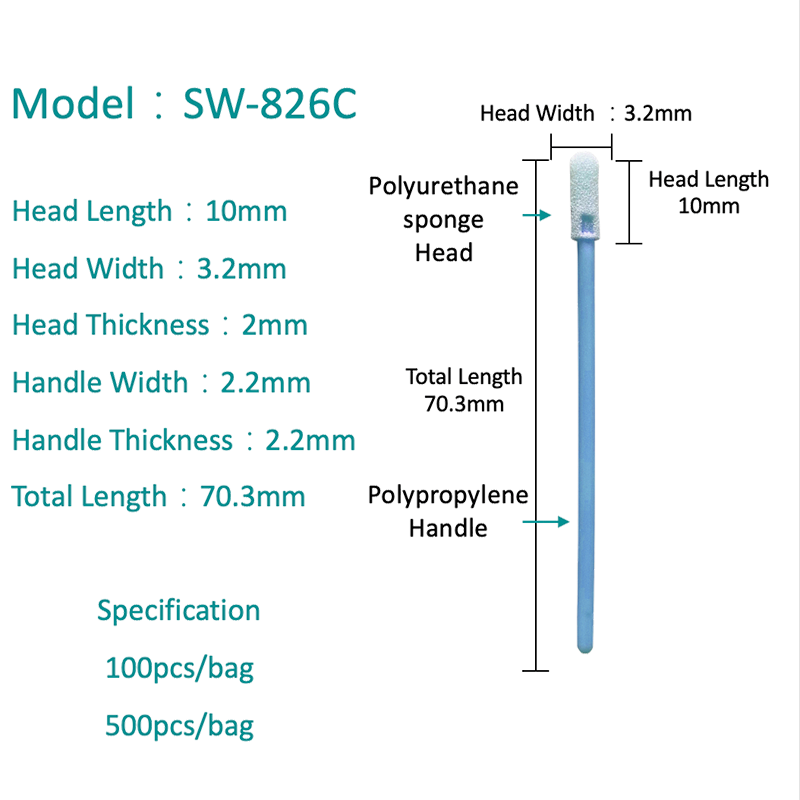
For instance, while both are synthetic, a polyester tip is excellent for general cleaning, but a polyurethane foam tip is superior for absorbing larger volumes of solvent and conforming to irregular surfaces.
| Tip Material | Primary Characteristics | Ideal Use Cases |
|---|---|---|
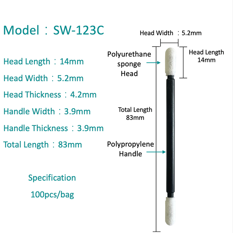
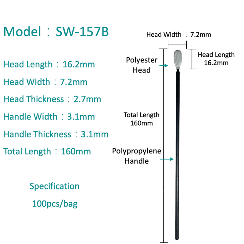
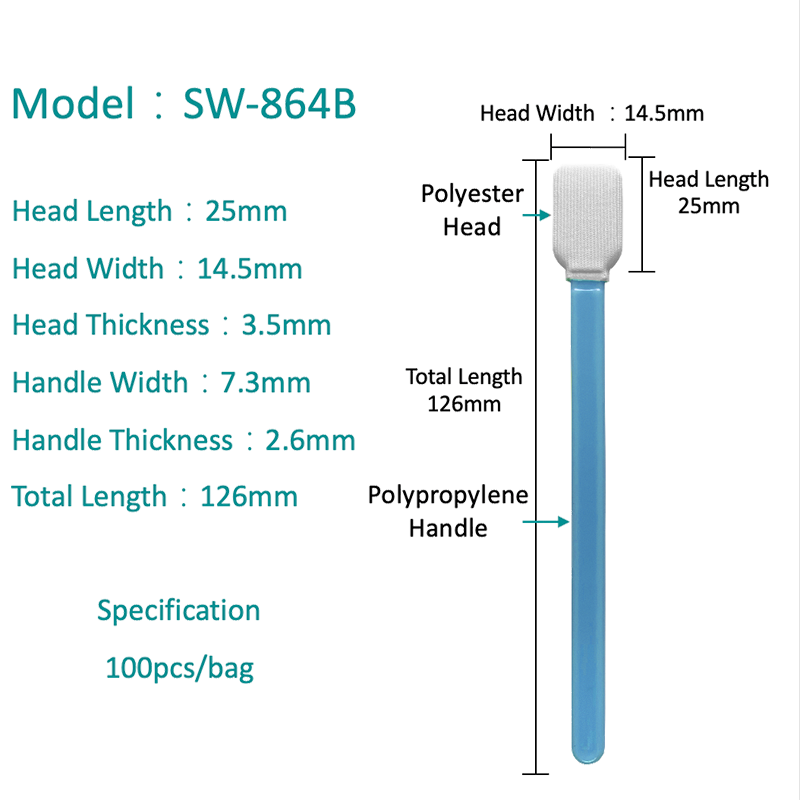
| Polyester | Low-lint, highly durable, good solvent resistance | General purpose cleaning, removing flux residues |
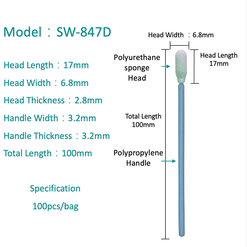
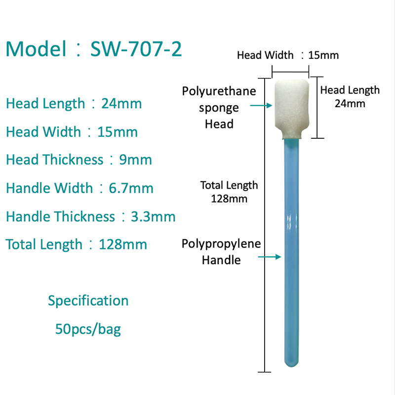
| Polyurethane Foam | Highly absorbent, soft, conforms to surfaces | Applying solvents, cleaning uneven components |
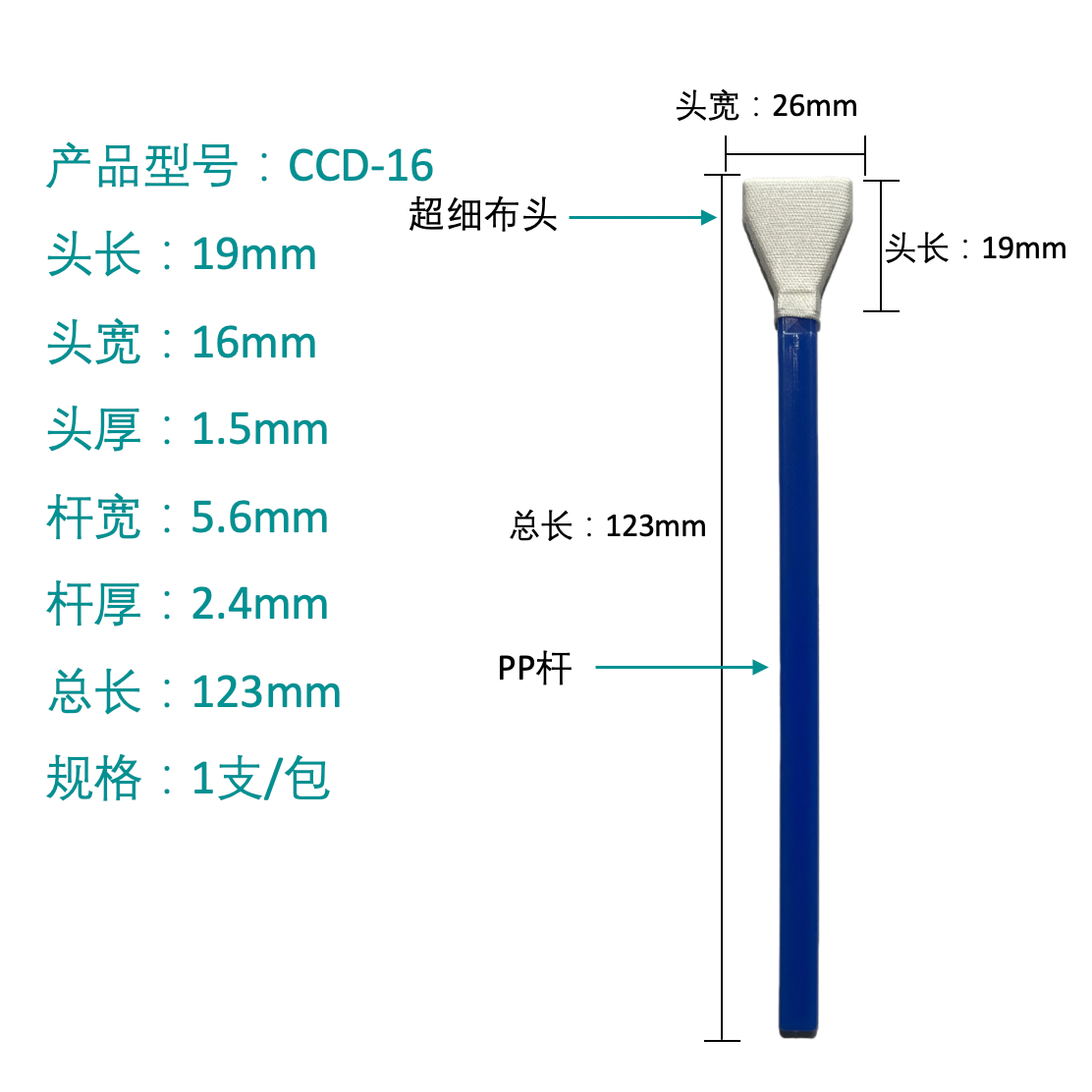
| Microfiber | Exceptional particle entrapment, very soft | Final wipe-downs, optical and laser cleaning |
Handle and Shaft Configurations
- Polypropylene Handles: Cost-effective and chemically resistant.
- Wooden Handles: Avoid in cleanrooms as they can splinter and shed particles.
- Long, Thin Shafts: Provide access to tight spaces and deep within assemblies.
Selecting the Right Swab for Your PCB Application
The process of selecting the right swab for PCB assembly involves matching the swab's properties to the specific cleaning challenge.
Key Selection Criteria
- Contaminant Type: Is it particulate, ionic, or organic flux?
- Component Sensitivity: How fragile are the parts being cleaned?
- Cleaning Solvent: Is the swab material compatible with the chemical used?
- Cleanroom Class: Does the swab meet the required cleanliness standard?
Application-Specific Recommendations
For Flux Removal
Use high purity solvent resistant cleaning swabs with a polyester tip, which can withstand aggressive flux removers without breaking down.
For Delicate Components
Opt for anti static swabs for precision cleaning with a soft foam tip to prevent scratching or damaging tiny solder joints.
The Manufacturing Edge: Why Cleanroom Production Matters
The environment where swabs are made is as critical as their design. Swabs labeled as cleanroom manufactured PCB swabs undergo a rigorous production process to ensure ultra-low levels of contamination. Suzhou Zhuojing Dust-free Technology Co., Ltd. leverages its Class 10 to Class 1000 cleanrooms and ultra-pure 18 mega-ohm water cleaning processes to guarantee that every swab is vacuum-sealed in a state of high purity, ready for the most sensitive environments in semiconductors, aerospace, and pharmaceuticals.
Best Practices for Using PCB Cleaning Swabs Effectively
Proper technique maximizes cleaning efficiency and minimizes the risk of damage.
- Always use a fresh swab for each cleaning session to avoid cross-contamination.
- Gently saturate the swab tip with the appropriate solvent—do not oversaturate.
- Wipe with gentle pressure, using a rolling motion to lift and trap contaminants.
- For optimal ESD safety, always use low lint static free swabs for electronics in conjunction with a grounded wrist strap.
Frequently Asked Questions (FAQ)
1. What is the main difference between a standard cotton swab and a professional PCB cleaning swab?
Professional PCB cleaning swabs are designed to be low-linting and static-dissipative, whereas standard cotton swabs shed fibers and can generate static electricity, posing a significant risk of damaging sensitive electronic components.
2. Can I use the same swab with different cleaning solvents?
It is not recommended. A swab's material is tested for compatibility with specific solvents. Using a high purity solvent resistant cleaning swab with an incompatible chemical can cause the tip to degrade, leaving residue on the PCB.
3. Why is the cleanroom manufacturing process so important for these swabs?
Cleanroom manufacturing, as practiced at our facilities, ensures that cleanroom manufactured PCB swabs are free from particulate, ionic, and microbial contaminants that could otherwise be transferred to your PCB, causing latent failures.
4. How do I choose between a polyester and a foam tip swab?
Choose polyester for durable, abrasive action on tough contaminants like hardened flux. Choose foam for a softer, more absorbent touch on delicate components or for applying solvents, making them a key tool among anti static swabs for precision cleaning.
5. What does "low lint" and "static free" mean in the context of low lint static free swabs for electronics?
"Low lint" means the swab tip is constructed from materials that minimize fiber shedding. "Static free" means the swab is made from materials that dissipate electrostatic charge, preventing a sudden discharge that can harm integrated circuits.


 English
  中文简体
中文简体 
